

Where is the way to go when perovskite batteries are commercialized?
The unremitting efforts of interface passivation make the VOC of perovskite halide battery reach 95.8% of the fine balance limit, which matches the 95.9% value of GaAs battery. However, the FF and short circuit current density (JSC) of halide perovskite are only 93.8% and 93.2% of the fine equilibrium limit, respectively, which are lower than those of Si and GaAs with > 95%. To overcome these limitations, the following work will be needed: (1) to eliminate the cross interface transmission loss in halide perovskite solar cells( 2) The internal quantum efficiency of the halogenated perovskite film is increased to 100% to increase the JSC and FF by 95% above the limit value. This is particularly important for wider band gap perovskite compositions, which are used as top cells in stacked photovoltaic systems, which are far from their radiation limits.
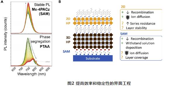
Up to now, efficient halide perovskite batteries only rely on Passivating one perovskite interface. The combination of Sam and 2D halide perovskite passivates the bottom and top interfaces, respectively, which makes it possible for both FF and JSC to approach their limits (Fig. 2b). However, in order to surpass the latest technology level, we need to better control the passivation layer and understand the mechanism of charge extraction.
Speed, stability and toxicity of perovskite production
Mass production speed
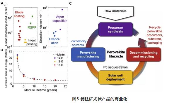
Although single junction perovskite solar cells with efficiency > 25% have been successfully fabricated, the effective area is only about 0.1 cm2. To achieve gigawatt scale perovskite production, millions of square meters of batteries will need to be deposited every year. This not only requires the development of deposition methods that can grow uniform and high-quality films on modules with an area of > 100 cm2, but also speed is a necessary consideration. Processing speed will affect the number of modules that can be processed per manufacturing hour, and improving processing speed is very important to reduce capital intensity, module manufacturing cost and lcoe. Therefore, large area solution processing methods (e.g., scraper coating, inkjet printing, slit coating, screen printing, and gravure printing) have attracted much attention due to their high-throughput volume to volume compatibility with environmental conditions( Figure 3a)
Directional radiation limit
The unremitting efforts of interface passivation make the VOC of perovskite halide battery reach 95.8% of the fine balance limit, which matches the 95.9% value of GaAs battery. However, the FF and short circuit current density (JSC) of halide perovskite are only 93.8% and 93.2% of the fine equilibrium limit, respectively, which are lower than those of Si and GaAs with > 95%. To overcome these limitations, the following work will be needed: (1) to eliminate the cross interface transmission loss in halide perovskite solar cells( 2) The internal quantum efficiency of the halogenated perovskite film is increased to 100% to increase the JSC and FF by 95% above the limit value. This is particularly important for wider band gap perovskite compositions, which are used as top cells in stacked photovoltaic systems, which are far from their radiation limits.
Up to now, efficient halide perovskite batteries only rely on Passivating one perovskite interface. The combination of Sam and 2D halide perovskite passivates the bottom and top interfaces, respectively, which makes it possible for both FF and JSC to approach their limits (Fig. 2b). However, in order to surpass the latest technology level, we need to better control the passivation layer and understand the mechanism of charge extraction.
Speed, stability and toxicity of perovskite production
Mass production speed
Although single junction perovskite solar cells with efficiency > 25% have been successfully fabricated, the effective area is only about 0.1 cm2. To achieve gigawatt scale perovskite production, millions of square meters of batteries will need to be deposited every year. This not only requires the development of deposition methods that can grow uniform and high-quality films on modules with an area of > 100 cm2, but also speed is a necessary consideration. Processing speed will affect the number of modules that can be processed per manufacturing hour, and improving processing speed is very important to reduce capital intensity, module manufacturing cost and lcoe. Therefore, large area solution processing methods (e.g., scraper coating, inkjet printing, slit coating, screen printing, and gravure printing) have attracted much attention due to their high-throughput volume to volume compatibility with environmental conditions( Figure 3a)
Directional radiation limit
The unremitting efforts of interface passivation make the VOC of perovskite halide battery reach 95.8% of the fine balance limit, which matches the 95.9% value of GaAs battery. However, the FF and short circuit current density (JSC) of halide perovskite are only 93.8% and 93.2% of the fine equilibrium limit, respectively, which are lower than those of Si and GaAs with > 95%. To overcome these limitations, the following work will be needed: (1) to eliminate the cross interface transmission loss in halide perovskite solar cells( 2) The internal quantum efficiency of the halogenated perovskite film is increased to 100% to increase the JSC and FF by 95% above the limit value. This is particularly important for wider band gap perovskite compositions, which are used as top cells in stacked photovoltaic systems, which are far from their radiation limits.
Up to now, efficient halide perovskite batteries only rely on Passivating one perovskite interface. The combination of Sam and 2D halide perovskite passivates the bottom and top interfaces, respectively, which makes it possible for both FF and JSC to approach their limits (Fig. 2b). However, in order to surpass the latest technology level, we need to better control the passivation layer and understand the mechanism of charge extraction.
Speed, stability and toxicity of perovskite production
Mass production speed
Although single junction perovskite solar cells with efficiency > 25% have been successfully fabricated, the effective area is only about 0.1 cm2. To achieve gigawatt scale perovskite production, millions of square meters of batteries will need to be deposited every year. This not only requires the development of deposition methods that can grow uniform and high-quality films on modules with an area of > 100 cm2, but also speed is a necessary consideration. Processing speed will affect the number of modules that can be processed per manufacturing hour, and improving processing speed is very important to reduce capital intensity, module manufacturing cost and lcoe. Therefore, large area solution processing methods (e.g., scraper coating, inkjet printing, slit coating, screen printing, and gravure printing) have attracted much attention due to their high-throughput volume to volume compatibility with environmental conditions( Figure 3a)
 Service life of perovskite components
At present, the main focus of perovskite field is efficiency. However, the technical and economic analysis shown in Fig. 3B shows that compared with the module life, changing the efficiency of perovskite single junction PV module from 14% to 18% has little effect on lcoe. Stability will play a central role in future commercialization efforts. Therefore, great efforts have been made to go beyond the thermodynamic instability of mapbi3 and develop more stable halogenated perovskites. In addition to thin films, more efforts are needed to develop packaging materials for perovskite modules and accelerated degradation testing protocols for perovskite.
Alleviating toxicity challenges in perovskite module life cycle
Recently, some progress has been made in reducing the risks associated with lead toxicity throughout the life cycle of perovskites, as shown in Figure 3C. For example, iron hydroxyapatite composites can absorb and separate lead from contaminated polar solvents such as fresh water. In addition to the hazards of lead, the solvents used in perovskite manufacturing (e.g., N, N-dimethylformamide) may be more dangerous than lead itself. Therefore, future work should focus on the development of large-area manufacturing processes using benign solvents, such as dimethyl sulfoxide, or solvent-free methods, such as rapid vapor deposition.
In a word, remarkable progress has been made in the field of pbhalide perovskite photovoltaic in a short time. At present, the performance of single junction polycrystalline perovskite cell is close to that of single crystal silicon cell. At the same time, perovskite batteries are now in the peak period of transferring from laboratory to market. In order to reach the radiation limit of perovskite solar cells and commercialize the technology, we need to develop it at the nanometer level, interface level, device and module level. In particular, understanding the role of impurities and extended defects, as well as developing more effective passivation interface methods, will be the key to push the efficiency to the radiation limit. For commercialization, we need to shift the focus from efficiency to rapid scale manufacturing, improve module life and develop technology to reduce the toxicity risk of perovskite in its life cycle. Overcoming these bottlenecks will enable halide perovskite solar cells to meet the urgent need of rapidly accelerating photovoltaic deployment.
This information is from the Internet for academic exchange only. If there is any infringement, please contact us to delete it immediately
18915694570
Previous: Qu Xiaogang Angew from